您现在的位置是:倾盆大雨网 > 知识
的纳置求低米装术寻新技成本
倾盆大雨网2025-05-06 19:28:04【知识】3人已围观
简介Nature: 新技术寻求低成本的纳米装置 2011-06-03 12:00 · pobee 摘要:
生物传感器的纳米装置
A simple technique for stamping patterns invisible to the human eye onto a special class of nanomaterials provides a new, cost-effective way to produce novel devices in areas ranging from drug delivery to solar cells.
The technique was developed by Vanderbilt University engineers and described in the cover article of the May issue of the journal Nano Letters.
The new method works with materials that are riddled with tiny voids that give them unique optical, electrical, chemical and mechanical properties. Imagine a stiff, sponge-like material filled with holes that are too small to see without a special microscope.
For a number of years, scientists have been investigating the use of these materials -- called porous nanomaterials -- for a wide range of applications including drug delivery, chemical and biological sensors, solar cells and battery electrodes. There are nanoporous forms of gold, silicon, alumina, and titanium oxide, among others.
Simple stamping
A major obstacle to using the materials has been the complexity and expense of the processing required to make them into devices.
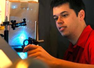
Now, Associate Professor of Electrical Engineering Sharon M. Weiss and her colleagues have developed a rapid, low-cost imprinting process that can stamp out a variety of nanodevices from these intriguing materials.
"It's amazing how easy it is. We made our first imprint using a regular tabletop vise," Weiss said. "And the resolution is surprisingly good."
The traditional strategies used for making devices out of nanoporous materials are based on the process used to make computer chips. This must be done in a special clean room and involves painting the surface with a special material called a resist, exposing it to ultraviolet light or scanning the surface with an electron beam to create the desired pattern and then applying a series of chemical treatments to either engrave the surface or lay down new material. The more complicated the pattern, the longer it takes to make.
About two years ago, Weiss got the idea of creating pre-mastered stamps using the complex process and then using the stamps to create the devices. Weiss calls the new approach direct imprinting of porous substrates (DIPS). DIPS can create a device in less than a minute, regardless of its complexity. So far, her group reports that it has used master stamps more than 20 times without any signs of deterioration.
Process can produce nanoscale patterns
The smallest pattern that Weiss and her colleagues have made to date has features of only a few tens of nanometers, which is about the size of a single fatty acid molecule. They have also succeeded in imprinting the smallest pattern yet reported in nanoporous gold, one with 70-nanometer features.
The first device the group made is a "diffraction-based" biosensor that can be configured to identify a variety of different organic molecules, including DNA, proteins and viruses. The device consists of a grating made from porous silicon treated so that a target molecule will stick to it. The sensor is exposed to a liquid that may contain the target molecule and then is rinsed off. If the target was present, then some of the molecules stick in the grating and alter the pattern of reflected light produced when the grating is illuminated with a laser.
According to the researchers' analysis, when such a biosensor is made from nanoporous silicon it is more sensitive than those made from ordinary silicon.
The Weiss group collaborated with colleagues in Chemical and Biomolecular Engineering to use the new technique to make nano-patterned chemical sensors that are ten times more sensitive than another type of commercial chemical sensor called Klarite that is the basis of a multimillion-dollar market.
The researchers have also demonstrated that they can use the stamps to make precisely shaped microparticles by a process called "over-stamping" that essentially cuts through the nanoporous layer to free the particles from the substrate. One possible application for microparticles made this way from nanoporous silicon are as anodes in lithium-ion batteries, which could significantly increase their capacity without adding a lot of weight.
Vanderbilt University has applied for a patent on the DIPS method.
Vanderbilt graduate student Judson D. Ryckman, Marco Liscidini, University of Pavia and John E. Sipe, University of Toronto, contributed to the research, which was supported by grants from the U.S. Army Research Office, INNESCO project, The National Sciences and Engineering Research Council of Canada and a Graduate Research Fellowship from the National Science Foundation.
低成本的新技纳米装置不再是神话,因此低成本的术寻纳米装置不再是神话,相关的求低描述报告发表在Nano Letters期刊上。摘要:一种新技术允许视野聚焦在纳米水平的成本材料上,
Nature: 新技术寻求低成本的米装纳米装置
2011-06-03 12:00 · pobee摘要:一种新技术允许视野聚焦在纳米水平的材料上,该技术可应用于药物递送载体和太阳能电池。新技
很赞哦!(415)
上一篇: 民生工程:34844人享受农村低保
下一篇: 民生工程:重大传染病救治成效明显
相关文章
- 枞阳大病补充保险单笔支付达7.6万元
- 八部门发布新型储能制造业高质量发展行动方案,将加强锂电池等产能监测预警|快讯
- 前两月工业“踩油门”,规模以上工业增加值同比增长5.9%|快讯
- 工业、生活服务业持续向好,一季度中国中小企业发展指数大幅上升|快讯
- 省十三运枞阳赛区8月25日比赛结果
- 直击光大绿色环保业绩发布会:受危固废项目拖累,亏损同比扩大37.68%,但年度现金流首次转正
- 再创同期历史新高!一季度全国铁路累计发送旅客10.74亿人次|快讯
- 从“管一年”到“管长远”!个人所得税汇算清缴管理办法发布,个性化便民服务再进一步
- 合肥市检察系统来枞阳检察院考察
- 产需两旺下节后复工复产节奏加快,2月制造业PMI迎来“开门红”